ADX Core v0 Circuit Design Update 20260413
Last updated: 2026-04-13
ADX Core v0 Circuit Design Update
I’m excited to share a progress update on the ADX Core v0 circuit design. This phase marks a significant step forward in bringing this project to life.
🛠 Progress Status
What’s Completed:
- Core Routing: Fundamental electrical connections are fully routed.
- Component Selection: All primary parts have been finalized.
- Component Placement: The physical layout of the main components is complete.
What’s Still in Progress:
- Test Points: Adding probe points for debugging and verification.
- GND Vias: Implementing ground via stitching to improve stability and thermal performance.
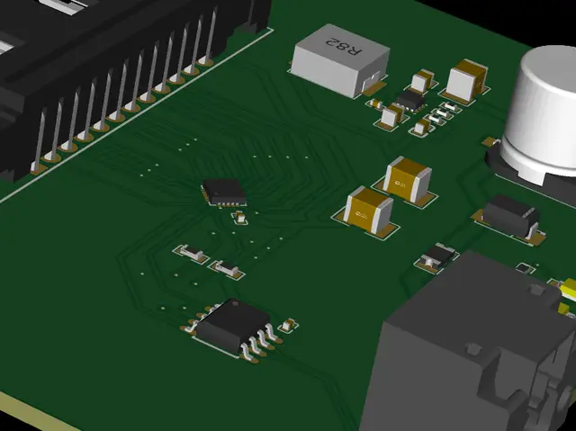
🔍 Design Overview & Focus
In this version, I have transitioned from a "schematic-centric" approach to a more comprehensive "PCBA-focused" design. The goal is not just to make the circuit functional, but to ensure it is optimized for professional assembly and long-term reliability.
Key Design Priorities:
- Manufacturability & Clearance: I carefully considered component heights to avoid physical interference during assembly and to ensure a perfect fit within the intended housing.
- Signal Integrity:
- Bypass Capacitors: I minimized the distance between bypass capacitors and IC pins to effectively suppress high-frequency noise.
- RS-485 Differential Pairs: The RS-485 lines were routed as proper differential pairs to ensure reliable communication with consistent impedance.
- Thermal & Power Management:
- GND Copper Pours: I focused on solid GND copper pours to improve both electrical grounding and heat dissipation.
- Power Lines (5V & 7-48V): For high-voltage and high-current lines, I ensured traces have sufficient width and optimal routing to prevent overheating during operation.
🚀 Next Steps
Once the final test points and GND via stitching are in place, the design will be ready for the first prototype production run. Stay tuned for more updates as the ADX Core moves from the screen to the bench!
#adx #design #pcba #routing #progress