ADX Core v0 Design Review (Failed)
ADX Core v0 Design Review (Failed)
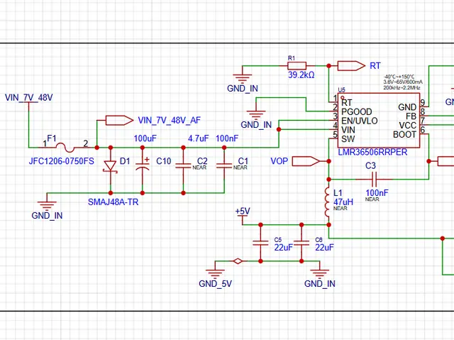
ADX Core V0, DCDC schematic
Terminal Block Section
When co-locating RS-485 and 48V power lines, conventional industrial cabling often suggests moving from a 2x2 to a 2x3 layout to include an NC (No-Connect) zone for better isolation.
However, ADX utilizes Ethernet cables. Since Ethernet is designed to handle PoE (up to ~57V) alongside data, and because introducing an NC zone would require untwisting pairs and stripping shields—potentially compromising signal integrity—I have opted for a 2x2 layout. Compared to standard industrial wire, Ethernet cabling poses a lower risk of shorts caused by stray wire strands. By using ferrule terminals for proper crimping, this risk is minimized enough to safely maintain the 2x2 configuration.
DC-DC Converter Section
The expansion board has a current consumption of approximately 500mA.
- ATtiny1616: Approx. 10.2mA (at 5V, 20MHz full operation)
- THVD24x0 (RS-485): Max 5.6mA (no load) + RS-485 bus drive current (up to 60mA absolute max rating)
Stability Considerations (The CFF Dilemma)
With the expansion board drawing 500mA and the mainboard MCU/RS-485 transceivers drawing several dozen mA, the total system current reaches nearly 90% of the maximum rating (600mA). The load fluctuates significantly from deep sleep (µA range) to peak load (approx. 560mA total).
Decision: To ensure stability under these high-load transients, I will modify the design to include a 22pF, C0G, 50V capacitor as a Feed-Forward Capacitor (CFF).
Review Suspension & Next Steps
- Complete Layout Overhaul: I have identified the need for a full PCB layout revision to improve manufacturability.
- Clearance Optimization: To ensure assembly reliability and follow DFM (Design for Manufacturing) standards, I will re-draw the component placement from scratch, focusing on maintaining a clearance equivalent to 1H (component height).
#adx #adxcore #design #pcba #review