ADX Development Log, Unifying Debugging UX and Circuit Architecture
ADX Development Log: Unifying Debugging UX and Circuit Architecture
In the development of ADX, we recently faced a challenge: how to balance robust power delivery with a seamless debugging experience. By aligning our hardware specifications with the practicalities of field debugging, we have arrived at a design that integrates UX directly into the circuit logic.
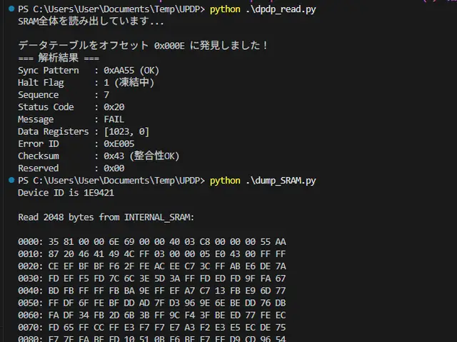
Dumping SRAM from the ADX prototype using Microchip’s Python and pymcuprog.
Key Conclusions
After a thorough technical evaluation, we have finalized the following specifications:
- DC-DC Output: Adjusted to 5.3V max, protected by a 1A-rated diode.
- Debug Interface: A 3-pin header (UPDI, VDD, GND) with a dedicated 1A-rated diode on the VDD receiving side.
- Power Architecture: The DC-DC and Debug VDD diodes remain separate, forming a Diode-OR circuit to prevent back-feeding.
- Processor Clock: The ATtiny1616-MNR is officially specified at 16MHz.
- The Result: No proprietary hardware is required for debugging; developers can use off-the-shelf USB-to-Serial UPDI boards.
Technical Background
1. The Challenge of UPDI Debugging
The primary goal was to establish an efficient UPDI debugging workflow for ADX. While our prototype supported sketch flashing via CH340E (USB Type-C), we needed a way to retrieve real-time logs similar to Serial.print.
The ATtiny1616 (1-series) used in ADX does not support the native serial-over-UPDI features found in the newer 2-series. We considered switching to the 2-series but ruled it out due to cost, size, and supply chain availability.
We experimented with the pymcuprog library to read SRAM data directly. However, we found that pymcuprog halts the CPU to access memory, making it impossible to monitor data in real-time while the application is running. Since ADX’s hardware TX/RX pins are dedicated to an RS-485 transceiver, we were left with limited options for standard serial output.
2. Physical UX: The 3-Pin Solution
We decided to separate the UPDI interface from the general-purpose GPIO. To keep the board stackable and low-cost, we settled on a 2.54mm pitch right-angle 3-pin header. This provides a secure physical connection that fits the ADX form factor and remains accessible even when expansion boards are stacked.
3. The Voltage Drop Dilemma (USB 4.7V vs. VDD)
A critical hurdle was the potential voltage drop when powering the board via USB. A standard USB voltage rail can dip as low as 4.7V. ADX, including expansion boards, can pull up to 600mA.
When using a Diode-OR circuit to prevent power contention between the onboard DC-DC and the USB debug power, we must account for the forward voltage drop V_f of the diodes. A 1A-rated Schottky diode typically drops about 0.6V.
- USB Supply: 4.7V (Min) - 0.6V (Drop) = 4.1V
Running the ATtiny1616 at 20MHz requires a minimum of 4.5V. At 4.1V, the system becomes unstable. While we can boost the onboard DC-DC output to 5.3V to compensate, we cannot control the voltage output of a user's generic USB-UPDI adapter.
4. Defining 16MHz as a Fixed Specification
Previously, 16MHz was a "recommended" setting for stability and thermal management. However, this power conflict turned 16MHz into a fixed specification.
By locking the clock at 16MHz, the ATtiny1616 operates reliably down to much lower voltages. This allows us to use standard 1A diodes and—most importantly—enables developers to use generic USB-UPDI adapters without needing a specialized 5.3V boosted debug jig.
Summary
By optimizing for a rock-solid 16MHz specification, we gained compatibility with standard USB power and off-the-shelf debugging tools. Sometimes, the best "User Experience" for a developer is simply ensuring the hardware works with the tools they already have.
#adx #arduino #embedded #atmel #attiny #circuitdesign #UPDI