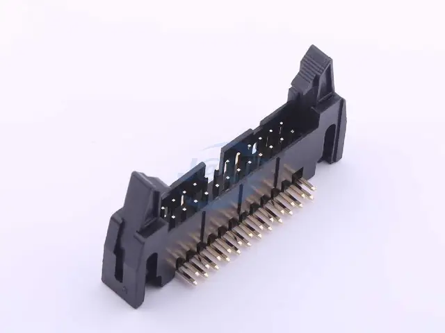
Design Analysis, 24 Pin Expansion Interface
Design Analysis: 24-Pin Expansion Interface for ATtiny1616
1. Overview
This document outlines the design strategy for a 24-pin external expansion interface on an ATtiny1616-based system. The primary objective is to ensure signal integrity and electrical stability when using standard 1.27mm pitch ribbon cables.
2. Design Methodology
The pinout was derived using a minimalist optimization approach, focusing on three core constraints:
- Electrical Capacity: Preventing voltage drops under peak loads (500mA) by utilizing parallel pins.
- Signal Isolation: Implementing a Ground-Signal-Ground (G-S-G) structure to mitigate crosstalk and EMI.
- Pin Efficiency: Every pin is assigned a specific functional or protective role; no pins are left unassigned or floating.
3. Pin Assignment and Rationale
| Pin | Signal | MCU Pin | Function / Rationale |
|---|---|---|---|
| 1, 2 | +5V | - | Power Supply. Parallel configuration to minimize voltage drop at 500mA. |
| 3 | GND | - | Power Isolation. Separation of power and signal domains. |
| 4 | UPDI | PA0 | Programming. Positioned to provide physical separation between power rails and the I2C bus. |
| 5 | GND | - | I2C Shield (Low). Isolates UPDI noise from the I2C bus. |
| 6 | SDA | PB1 | I2C Data. |
| 7 | GND | - | Internal Bus Shield. Prevents mutual interference between SDA and SCL. |
| 8 | SCL | PB0 | I2C Clock. Flanked by GND pins for maximum noise protection. |
| 9 | GND | - | Domain Boundary. Digital-to-Analog noise isolation. |
| 10 | DAC OUT | PA6 | Precision Analog. Isolated by GND (9, 11) to maintain signal purity. |
| 11 | GND | - | Analog Shield. Isolation from general-purpose I/O signals. |
| 12 | AC0/GPIO | PA7 | Comparator Output / General Purpose I/O. |
| 13 | AIN/GPIO | PA3 | Analog Input / General Purpose I/O. |
| 14 | GND | - | Analog Internal Shield. Crosstalk reduction between multiple inputs. |
| 15, 16 | AIN/GPIO | PB4, PB5 | Analog Input / General Purpose I/O. |
| 17 | GND | - | Domain Boundary. Analog-to-SPI noise isolation. |
| 18-20 | SPI | PC3-PC1 | SS / MOSI / MISO. |
| 23, 24 | GND | - | System Ground. Terminal shielding and reference stability. |
4. Firmware Implementation Requirements
To align with the hardware design, the following ATtiny1616 register configurations are required:
4.1 Peripheral Pin Mapping
Since the SPI bus is assigned to the PC port on the expansion header, the PORTMUX must be configured.
- Register:
PORTMUX.CTRLB - Setting: Set
SPI0bit to1to enable alternative pin mapping.
4.2 SPI Master Mode Stability
To prevent unintended transitions to Slave mode (mode fault conditions) when PC3 (SS) is pulled low:
- Requirement: Configure PC3 as an Output pin.
- Alternative: Set the
SSD(Slave Select Disable) bit inSPI0.CTRLBto1to disable hardware-level SS monitoring.
4.3 Input Buffer Management
For pins assigned to analog functions (PA6, PA7, PA3, PB4, PB5), the digital input buffers must be disabled to prevent shoot-through current and digital noise floor rise.
- Register:
PORTx.PINnCTRL - Setting:
INPUT_DISABLE(0x4).
4.4 I2C Interface Specifications
The internal pull-up resistors of the ATtiny1616 are typically insufficient for the capacitance and length of a 24-pin ribbon cable.
- Requirement: External pull-up resistors (2.2kΩ to 4.7kΩ) must be present on the peripheral/bus side to ensure reliable signal transitions.
5. Summary
The selection of a 24-pin interface is a direct result of prioritizing signal integrity over pin-count reduction. By treating GND placement as a structural component rather than a simple return path, this design achieves a robust communication environment suitable for industrial or high-noise applications.
#adx #design #ATtiny1616 #Hardware-Design #Firmware #Pinout #I2C #SPI